Yangtze Aiming For 8% Of NAND Output Next Year
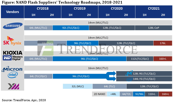
After submitting samples of TLC and QLC 128-layer NAND to controller chip suppliers in Q1, Yangtze Memory is aiming to start running wafers in Q3 and ramp to mass production in Q4, reports TrendForce.
After submitting samples of TLC and QLC 128-layer NAND to controller chip suppliers in Q1, Yangtze Memory is aiming to start running wafers in Q3 and ramp to mass production in Q4, reports TrendForce.

The initial applications being considered for the 128-layer process include UFS-based storage solutions and SSDs; Yangtze also intends to ship packaged dies and wafers to module houses.
From 2021, applications are expected to be extended to client SSDs, eMMC/UFS solutions, and other storage products.
This timetable means that Yangtze product could start impacting NAND prices in Q4, reckons TrendForce.
Yangtze is now focussed on improving yields and getting customer approvals.
With NAND ASPs dropping 46% last year, suppliers were moving into loss territory and trimmed capex and, consequently, 2020 output. This, believes Yangtze, has given it its chance to get established in the market.
Yangtze has one fab operational at Wuhan with another at Chengdu due to come on-stream this year . There are two more fabs being built on the Wuhan site.
Yangtze is aiming to get 8% of total NAND output next year.


